STTP 3: Mixed Signal VLSI Design
Topic 1: Memory Design: An Industry Perspective

Invited Speaker:
Dr. Abhishek Sharma
Components Research,
Intel Corporation, Oregon, USA
Brief Biography:
Abhishek A. Sharma completed his BE from Sardar Patel Institute of Technology in 2010 and completed his MS and PhD from Carnegie Mellon University in 2012 and 2015 respectively.
His thesis was centered around using new memory technologies for high bandwidth applications. He is currently engaged in memory research at Components Research, Intel, USA. His core research areas include co-optimization of device and design in memory arrays for high performance applications.
His core strengths are based on strong foundations and 9+ years of experience in novel transistor research and in cross-disciplinary device-circuit co-design, circuit-system interaction with special focus on using new technologies to enable high bandwidth connectivity for tightly connected compute-memory products.
Topic Keynote: Mixed Signal Circuits and Systems: Emerging Applications
Topic 2: Switch Capacitor Circuits
Invited Speaker:
Dr. Maryam Shojaei Baghini
Brief Biography:
Dr. Maryam Shojaei Baghini is Professor at Electrical Engineering Department Indian Institute of Technology Bombay. She did B. S. in Electrical Engineering from S. B. Univ. of Kerman, Ph.D. and M.S., both in Electrical Engineering from Sharif Univ. of Technology and Post Doc. Research at Dept. of Electrical Engineering, IIT-Bombay.
Dr. Maryam Shojaei Baghini received the Richard Feynman Prize in 2014, ICE (Institute of Civil Engineers), UK. She has 43 journal publications and 91 conference publications. She has 26 patents. She is co-author of the books „Applications of Evolutionary Algorithms in VLSI‟ and „Hardware Development of Wearable ECG Devices‟. More than 12 chips are fabricated and successfully tested by her. Her research interests are Technology-aware design (device circuit co-design), Integrated circuits and system design with emerging devices, Analog/Mixed-signal VLSI design and test, Specific technologies and performance-optimized analog/mixed-signal/RF circuits & systems for healthcare applications, Integrated power management for SOC applications, High-speed data transmission and interconnects, Circuit and system modeling/optimization, Circuit and system design with organic thin film components, RF/Microwave integrated circuit design, Analog aspects of digital circuits, Sensor-Circuit Integration and Analog/MixedSignal/RF EDA (CAD tools, theory and implementation).
Abstract:
Topic 1: A typical analog/mixed-signal system-on-a-chip (AMS-SoC) has a variety of components including digital processors, analog circuitry, radiofrequency (RF) circuitry, true mixed-signal circuitry integrated together to achieve cost and performance tradeoffs. In real-life applications mixed-signal designs are everywhere, for example, smart mobile phones. This keynote talk will feature on various emerging applications of Mixed-Signal Circuits.
Topic 2: Knowing the basics of switch capacitor circuits is very important for any CMOS Mixed Signal Circuit Designers. Switch capacitor circuits are the basic circuits that are used in design of various applications like data converters. This session will primarily be on fundamentals of Switch-Capacitor Circuits.
Topic: Device, Circuit and Architectures for enhancing Hardware Security
Invited Speaker:
Dr. Ramesh Vaddi
Associate Professor
Department of ECE
SEAS, SRM University, Amaravati, AP
Brief Biography:
Dr. Ramesh Vaddi completed Ph.D. in Microelectronics and VLSI from Indian Institute of Technology Roorkee, India in 2011. He was a Senior Research Fellow at National University of Singapore during 2018-19.
He was Postdoctoral Scholar at Pennsylvania State University, USA during 2013 and Postdoctoral Research Fellow in the School of Electrical and Electronic Engineering, Nanyang Technological University during, 2011 -2012. Dr. Vaddi has worked as an Assistant Professor in IIIT Naya Raipur and Shiv Nadar University, India and presently he is an Associate Professor in ECE Department at SRM University, Amaravati, AP. His research interests include Post-CMOS devices for energy efficient VLSI Designs, Hardware security for IoT, VLSI accelerators for AI Edge Computing. At Penstate, he was involved in the Semiconductor Research Corporation (SRC) sponsored projects “Centre for Low Energy Systems Technology (LEAST) and NSF sponsored Nanosystems Engineering Research Centre for Advanced Self-Powered Systems of Integrated Sensors and Technologies (ASSIST).
He has published research outcomes in several top IEEE conferences and peer reviewed International journals in the device and circuits society and has about 45 research publications and 2 USA patents to his credit. He held few visiting researcher appointments and invited talks at various globally reputed institutes such as Hong Kong University of Science and Technology and Missouri University of Science and Technology, Rolla, USA. Dr. Ramesh Vaddi has been a TPC member of various International Conferences/Symposiums such as VDAT, INIS and a reviewer of IEEE Trans. on BioCAS, IEEE Trans. on VLSI systems, IEEE Tran. On Electron Devices, IEEE Tran. On Electron Devices Letters, IEEE Tran. On Nanotechnology, Elsevier Microelectronics Journal, Journal of Applied Physics, IOP Semiconductor Science and Technology, etc, and Technical committee member of Several IEEE International conferences such as DAC, ISCAS, ISLPED, etc. He is an IEEE Senior Member and Fellow of IETE.
Topic 1: Full custom and Semi-Custom IC Design Flow Overview- Tool perspective
Topic 2: Synthesis and Pre-Layout STA
Topic 3: Physical Design & Verification flow – Industry perspective
- Demo : Logic Synthesis and Pre- Layout STA using Cadence Genus
Topic 4: Floor plan and Power plan & APR, Clock Tree Synthesis, Physical verification
- Demo: Getting started with Physical Design using Cadence Innovus
- Demo: Placement & Routing of an SoC using Cadence Innovus
- Demo: Power, Timing Analysis signoffs using Cadence Voltus and Tempus
Invited Speaker:
Mrs. Saraswati BP
PD Engineer,
Entuple Technologies, Bengaluru
Brief Biography:
Mrs. Saraswati BP, a Graduate with Bachelor of Technology in Electronics and Communication Engineering from Vivekananda Institute of Technology, Bangalore.
Currently working as PD Engineer for Cadence based at Bangalore carrying 3 years of
experience in handling various Cadence tools and the corresponding domains for training and support for Academic sector pan India.Worked as a Tech Support Engineer- Cadence Entuple Technologies Pvt Ltd (Sep 2017 to 2018)
Training in ASIC Physical Design and Verification with hands-on experience at Entuple
Technology Pvt Ltd.
Area of work deals with ASIC Physical Design and Verification, Synthesis, RTL Coding, Timing and Power Analysis along with considerable hand On experience with Full Custom IC Design flow.
Invited Speaker:
Mr. Sai Krishna P L N
Application Engineer
Entuple Technologies, Bengaluru
Brief Biography:
Graduate with Bachelor of Technology in Electronics and Communication Engineering from MLR Institute of Technology, Hyderabad.
Completed Training and Worked as Physical Design Engineer for 8 months at Entuple
Technologies Pvt Ltd, Bangalore.Currently working as Application Engineer for Cadence based at Bangalore carrying 2+ years of experience in handling various Cadence tools and the corresponding domains for training and support for Academic sector pan India. Area of work deals with ASIC Physical Design, Synthesis, RTL Coding and Timing Analysis along with considerable hand On experience with Full Custom IC Design flow.
Invited Speaker:
Mr. Navin Sankar
Field Application Engineer,
Entuple Technologies, Bengaluru
Brief Biography:
Mr. Navin sankar is working as a Field Application Engineer at Entuple Technologies, Bangalore since 2017 October. His role includes Logical & Physical Synthesis, PnR flow consisting of various steps such as Floorplan, Powerplan, Sanity Check, Placement, Clock Tree Synthesis (CTS), Routing and Design Optimization (preCTS, postCTS and postRoute).
Having experience of 2 years in the field of Application Engineering for EDA products. He has supported on some of the design related queries at different levels like RTL Design, RTL Synthesis, Physical Design, Physical Verification in PD flow.
He is also trained in ASIC Physical Design and Custom IC Design with hands-on experience in backend design flow including – Synthesis, Floor-planning, Power Planning, Placement, Clock Tree Synthesis, Routing, Static Timing Analysis (OCV, CPPR, Multi-cycle path), and Physical verification (DRC, LVS)
Topic: Secure Memory System Optimizations

Invited Speaker:
Mr. Prashant Nair
Assistant Professor,
Department of Electrical and Computer Engineering,
University of British Columbia
Brief Biography:
He received his Ph.D. and M.Sc. in Electrical and Computer Engineering from the Georgia Institute of Technology and the B.Engg degrees in Electronics Engineering from the University of Mumbai.
Prashant was a Post-Doctoral Researcher (Research Scientist) at IBM Thomas J. Watson Research Center in New York. Prashant’s interests are in the areas of reliability, security, and performance-power efficient memory systems. He is also interested in system-level and architecture-level optimization to enable efficient and practical quantum computers. He frequently publishes in several top-tier conferences like ISCA, MICRO, HPCA, and ASPLOS. Prashant has served as a primary reviewer for several major conferences in computer architecture, including ISCA, ASPLOS-2016, IEEE CAL, ACM-TACO, ACM-TC, and SBAC-PAD.
Topic: Data Converters: ADC and DAC
Invited Speaker:
Dr. S. Kumaravel
Associate Professor
Vellore Institute of Technology
Brief Biography:
Dr. S. Kumaravel is Associate Professor at Electronics Engineering Department Vellore Institute of Technology. He earned Ph.D. degree in from NIT TRICHY. He has published more than 26 papers in various journals and conferences. His area of interest are Mixed Signal Circuit Design, Low Power Design.
Abstract:
Data Conversion is the process of changing or converting one form of data in to another form. In processing and communication there are only two types of data forms i.e analog and digital data. The converter which converts the digital data in to analog data is called analog to digital to analog converter (ADC) and in the same the converter which converts digital to analog is called as DAC. Design of ADC and DAC is an evergreen topic of research. In this sessions basic architectures of ADC and DAC will be taught to the participants.
Topic: Dynamic Offset Cancellation Techniques
Invited Speaker:
Mr. Meraj Ahmed
Research Scholar, IIT Bombay
Brief Biography:
Mr. Meraj Ahmed did his M.Tech. in Microelectronics from IIT Bombay. His doctoral research at IIT Bombay is on CMOS analog and Mixed Signal VLSI Design. He was visiting research scholar at Nano Lab Tufts University. He is also the embedded system consultant.
Abstract:
At low frequencies, offset, 1/f noise and drift are the dominant error sources of operational amplifiers. This is especially true in CMOS technology. There are three types of CMOS offset cancellation techniques: trimming, chopping, and auto-zeroing. Trimming is usually performed during production to eliminate offset. Auto-zeroing is a sampling technique in which the offset is measured and then subtracted in subsequent clock phases. Chopping, on the other hand, is a continuous-time modulation technique in which the signal and offset are modulated to different frequencies. Due to the modulated offset and 1/f noise, a chopper ripple appears at the amplifier output. Since chopping and auto-zeroing are dynamic techniques that continuously reduce offset, they also remove low frequency 1/f noise as well as offset drift over temperature or time. This session is about details of dynamic offset cancellation techniques.
Topic: Low Power Architectures for Signal Processing and Communications

Invited Speaker:
Dr. Mohd. Hasan
Professor, AMU
Brief Biography:
Prof. Hasan has been working as a full Professor since March, 2005. He served as Chairman (HoD) of the Department from 12 Oct., 2015 to 11 Oct., 2018. He completed his PhD from the University of Edinburgh, UK on a Commonwealth Scholarship in the area of “Low Power Architectures for Signal Processing and Communications”.
He also worked as a Visiting Researcher on his own Royal Academy of Engineering, UK funded project on “Low Power FPGA’ in the same University. He has published 161 papers in refereed journals and conferences with 1401 citations, h-index=20 and i10 index=44. This also includes fifteen IEEE Transactions/Journals and 47 Scopus indexed journal publications. He received “Paper of the Year Award” by the Editors of the famous International ETRI Journal for his paper entitled “High Performance Low power FFT cores” along with a best International conference paper award. He has supervised eight PhDs and currently supervising four more along with many M.Tech. Dissertations. He has delivered several keynote addresses and invited talks in Conferences and Workshops. He has filed three patents on the design of magnetic RAM (MRAM) and one patent on robust SRAM. His research interests are in VLSI Design, Nanoelectronics, Ultra low power design, Spintronics, Battery-less electronics, Variability aware design. He is also a Senior member of IEEE.
Topic 1: Implementation of DSP Algorithms in VLSI

Invited Speaker:
Dr. Shaila Subbaraman
Retd. Professor
Walchand College of Engineering Sangli
Brief Biography:
Dr. Shaila Subbaraman obtained her M. Tech. from I.I.Sc. Bangalore in 75 She has done her Ph. D. in “Radiation and hot carrier effects in submicron MOS devices” from IIT Bombay in 1999. She served Walchand College of Engineering, Sangli from 1989.
She worked as resource person for various workshops/ short term courses/ guest lectures, Expert lectures on NBA and OBE guidelines at various colleges in Maharashtra She was deputed by NPIU for delivering guidelines on NBA and OBE. She was working as institute NBA/NAAC coordinator, Head of the Department and Dean Academics at Walchand College of Engineering, Sangli. She had Industry experience in various capacities (Engineer, Senior Engineer, Deputy Manager) for 14 years in semiconductor device/IC manufacturing industries in Pune. Her areas of research interest are: CMOS VLSI, Design, Digital System Engineering DSP-VLSI, CMOS VLSI Design, Analog VLSI Design, Testing and Testability.
Topic: Mind Power
Invited Speaker:
Dr. Jagbir Singh
Mental Conditioning Trainer and Sports Psychologist
Brief Biography:
Dr. Jagbir Singh has experience of over 21 years. He did his Doctorate of Philosophy in Sports Psychology from Yoga Samskrutham University-Florida, USA on ‘Impact of Rajyoga on Sports Performance’.
Presently he is coordinating the activities of Sports Wing of Rajyoga Education & Research Foundation at International Headquarters, Mt Abu, Rajasthan, India.
He has the distinction of winning Seven Gold Medals in A.F. Boxing in different weight categories in a row from 1987 to 1993. He represented Services Cycling Team in the Nationals 1993 at Mumbai (Sion) and participated in 25+ marathons. He won Gold Medal in 10m Air Rifle in Haryana State Shooting Championship 2002. He was sent to Rio Olympics 2016 in Brazil by Director General, Sports Authority of India (SAI), New Delhi to motivate Indian contingent.
He was invited as Honored Guest / Speaker at many events e.g. Afro-Asian Games, National Games, Beijing Olympic Games, Commonwealth Games etc. He was instrumental in organizing ‘Mind Power Training Sessions’ for Mumbai Cricket Team, National Shooting Team, Indian Women Hockey Team, Indian Women Cricket Team, National Badminton Team, National Body Building Team, North East Mount Everest Expedition, Rio Olympics and many more.
STTP 2: Analog CMOS Design
Chief Guest and Speaker for Valedictory Session

Invited Speaker:
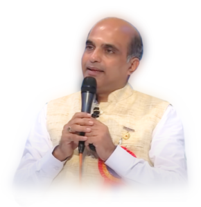
Mr. Pramoud Rao,
Promoter and Managing Director,
Zicom Electronic Security Systems
Brief Biography:
Mr. Rao has done Bachelor of Science(Honours) degree in Chemistry from Mumbai University. As the Managing Director for Zicom, he leads the innovation and strategic business to establish the name Zicom synonymous with electronic security. He oversees the growth of Zicom in all aspects. Be it finance, business development, admin or marketing. He is basically involved in the crucial business operations.
After merging Zicom’s integration business with Schneider Electric, he joined them as their Security Ambassador for the Asia-Pacific region during May 2010 to April 2012. Using his business experience, he helped them promote and create awareness about their foray into the eletronic security business. He also helped them setup their establishment, chart profitable market avenues, add value to their organization and help them grow in the APAC region.
He was the National President for Fire and Safety Association of India during April 2010 to March 2012. He proactively worked towards promoting the cause of safety and security across India. He helped businesses and organizations understand and value the criticality of security.
Topic: Keynote: Analog Design: An Industry Perspective

Invited Speaker:
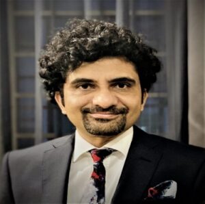
Mr. Aniruddha Satoskar
Design Engineer
Cirrus Logic, Austin, Texas, USA
Brief Biography:
He is skilled and experienced IC Design Engineer. Seasoned in Digital ASIC Design and Signal Processing hardware development. He is a proven innovator with 30+ US patents issued. Skills include: System modeling (Matlab/Simulink/System Verilog), Front-End RTL architecture and design, IP integration, Design Quality (Lint, CDC etc.) and Physical Design (synthesis and timing).
Currently he is design lead on multiple mixed-signal integrated circuit projects. He has successfully led teams of 10+ engineers on development of high volume ASIC’s such as the company’s flagship general market boosted amplifier product. Inventor on 30+ approved US patents on topics such as data converters, dynamic range enhancement, impedance detection and class H amplifiers. Experience working closely with Verification (UVM), Firmware, Validation (FPGA prototyping and Post silicon) and Product Test teams to resolve hardware issues. He is having an experience of supporting physical design team through back-end flow (synthesis, floor-planning, CTS, routing, STA, scan and MBIST insertion). Extensive experience on working with in-house and customer Marketing, Project Management and Systems teams for product definition and project status tracking. Proficient in architecting and implementing fixed-point DSP filters / algorithms and in the digital design and verification of mixed signal IP such as ADCs, DACs, PLL’s, boost converters etc. He is highly skilled in IP integration with in-depth understanding of various data and control protocols (inter and intra chip – I2C, SPI, I2S, TDM, HD Audio, Soundwire, APB and AHB protocols). He has architected and designed digital portion of flagship Analog-to-Digital Converter IP and worked on diverse signal processing IP’s such as decimation and interpolation filters, parametric equalizers, crossfaders, sample rate converters and delta sigma modulators. Also experienced in DSP core integration and in adaptive signal processing for noise and crosstalk cancellation.
Abstract: Analog design is challenging. There are many ways to get from input to output, and the circuitry in the middle can lead to divergent results. Analog design is like learning a language. The early days of analog design saw almost every component “handcrafted “to satisfy the designer of its suitability for the particular application.
Topic: Keynote: Analog CMOS Design
Invited Speaker:
Dr. Mohd. Hasan
Professor, AMU
Brief Biography:
Prof. Hasan has been working as a full Professor since March, 2005. He served as Chairman (HoD) of the Department from 12 Oct., 2015 to 11 Oct., 2018. He completed his PhD from the University of Edinburgh, UK on a Commonwealth Scholarship in the area of “Low Power Architectures for Signal Processing and Communications”.
He also worked as a Visiting Researcher on his own Royal Academy of Engineering, UK funded project on “Low Power FPGA’ in the same University. He has published 161 papers in refereed journals and conferences with 1401 citations, h-index=20 and i10 index=44. This also includes fifteen IEEE Transactions/Journals and 47 Scopus indexed journal publications. He received “Paper of the Year Award” by the Editors of the famous International ETRI Journal for his paper entitled “High Performance Low power FFT cores” along with a best International conference paper award. He has supervised eight PhDs and currently supervising four more along with many M.Tech. Dissertations. He has delivered several keynote addresses and invited talks in Conferences and Workshops. He has filed three patents on the design of magnetic RAM (MRAM) and one patent on robust SRAM. His research interests are in VLSI Design, Nanoelectronics, Ultra low power design, Spintronics, Battery-less electronics, Variability aware design. He is also a Senior member of IEEE.
Abstract: Many types of signal processing have indeed moved to the digital domain, analog circuits have proved fundamentally necessary in many of today’s complex, high performance systems. The design of analog circuits itself has evolved together with the technology and the performance requirements. As the device dimensions shrink, the supply voltage of integrated circuits drops, and analog and digital circuits are fabricated on one chip, many design issues arise that were unimportant only a decade ago. Such trends demand that the analysis and design of circuits be accomplished by an in-depth understanding. In this session, participants will be introduced to Analog CMOS Design, emphasizing fundamentals, as well as new paradigms. It is useful in to developing a solid foundation.
Topic-1: Analog Circuit Simulation
Topic-2: Post-Layout Simulation and LVS
Invited Speaker:
Dr. Naushad Alam
Assistant Professor
Department of Electronics Engineering
Aligarh Muslim University, Aligarh.
Brief Biography:
Naushad Alam received B. Tech. degree in Electronics & Communication Engineering from Jamia Millia Islamia, New Delhi in 2003, and M. Tech. Degree in Electronic Circuits & Systems Design from Aligarh Muslim University, Aligarh in 2009. He earned Ph.D. degree in Microelectronics from Indian Institute of Technology Roorkee, India in 2013.
His doctoral work was on nanoscale circuit design considering the impact of process-induced mechanical stress. He has published 25 papers in SCI indexed journals that include 10 IEEE Transactions and 33 papers in reputed conferences such as IEEE ISQED, IEEE ISCAS, IEEE TENCON, IWPSD, VDAT, IEEE ISED, IEEE UPCON etc. He has received four Best Paper Awards at ICSCI-2008, IMPACT-2013, VDAT-2015 and IMPACT 2017 respectively and delivered five invited talks at BIT Mesra (2014), MNIT Jaipur (2015), SPIT Mumbai (2015) and ZHCET Aligarh (2016) respectively. He has supervised one PhD thesis on Robust SRAM design and presently supervising three PhD students. He has also successfully executed a UGC funded research project on TFET based SRAM cell design for IoT Applications. His research interests include device-circuit co-design, robust nanoscale circuit design, low power circuit design, PVT tolerant circuit design, Near-Threshold/Sub-Threshold circuit design etc.
Topic-1: Analog Circuit Simulation
In this session, participants will be introduced to schematic based design entry, pre-layout simulation of CMOS logic circuits and measurement of performance metrics using SPICE simulations. Monte Carlo simulation and corner analysis of CMOS circuits will be demonstrated.
Topic-2: Post-Layout Simulation and LVS
In this session, participants will be introduced to physical/layout design of CMOS circuits, post-layout simulations and measurement of performance metrics using SPICE simulations. This will include Layout vs Schematic, Design Rule Checks and parasitic extraction etc. Comparison of pre-layout simulation and post-layout simulation will also be demonstrated.
Topic-1: Analog Circuit Design – Setting the Perspective
Topic-2: The gm/ Id technique – Design Flow Illustration
Topic-3: Illustrative Design of a 7 pack OPAMP – Spec to Schematic Deisgn Sign Off
Topic-4: A Brief Introduction to Analog Layout Concepts
Topic-5: Illustrative Layout Design of the 7 pack OPAMP
Topic-6: Custom Digital IC Design – Illustrative Design of A CMOS Inverter Standard Cell
Invited Speaker:
Mr. Sijo Thomas
Design Engineer Analog/RF
Entuple Technologies, Bengaluru
Brief Biography:
Mr. Sijo Thomas is currently working at Entuple Technologies India Pvt. Ltd., Bangalore in the capacity of Design Engineer – Analog/ RF IC as a member of the Custom IP Development Team and involved in the design and development of Analog/ RF IP blocks for in-house/client requirements.
Experienced Analog/RFIC design specialist with a demonstrated history of working in the electrical and electronic manufacturing industry with experience in 45nm and below. Skilled in Analog Mixed Signal Circuit Design, RF IC Design, IC Design flow. Strong background in CMOS process, network analysis, single stage to multi-stage amplifiers. Completed Master of Technology (M.Tech.) focused in VLSI DESIGN from SRM Institute of Science & Technology, Chennai. His area of expertise includes RFIC designs such as LNA, PA, VCO and, power management blocks such as BGR & LDO, current references, OPAMPs & ADC. Supported layout engineers for various amplifier circuits, including physical verification upto parasitic extraction.
Tools: cadence virtuoso, spectre/spectre RF, virtuoso layout xl, ADE XL/GXL, ADE Explorer/Assembler, ADS, ANSYS HFSS
Topic 1 : Analog Circuit Design – Setting the Perspective
Topic 2 : The gm/ Id technique – Design Flow Illustration
Invited Speaker:
Mr. Venugopal D. Kulkarni
Consultant – AMS Circuits and Systems Design/ Training,
Entuple Technologies, Bengaluru
Brief Biography:
Mr. Kulkarni has completed M.Tech in Microelectronics from IIT Bombay . He is working as consultant since May 2014.
He has experience of working with coreEL Technologies, Bengaluru for 3 years. He has also worked as Dean Sandeepai Scool of Embedded System Design for 3 years.
Topic 1: The gm/ Id technique – Design Flow Illustration
Topic 2: Illustrative Design of a 7 pack OPAMP – Spec to Schematic Design Sign Off
Topic 3: A Brief Introduction to Analog Layout Concepts
Topic 4: Illustrative Layout Design of the 7 pack OPAMP
Invited Speaker:
Mr. Navin Sankar
Field Application Engineer,
Entuple Technologies, Bengaluru
Brief Biography:
Mr. Navin sankar is working as a Field Application Engineer at Entuple Technologies, Bangalore since 2017 October. His role includes Logical & Physical Synthesis, PnR flow consisting of various steps such as Floorplan, Powerplan, Sanity Check, Placement, Clock Tree Synthesis (CTS), Routing and Design Optimization (preCTS, postCTS and postRoute).
Having experience of 2 years in the field of Application Engineering for EDA products. He has supported on some of the design related queries at different levels like RTL Design, RTL Synthesis, Physical Design, Physical Verification in PD flow.
He is also trained in ASIC Physical Design and Custom IC Design with hands-on experience in backend design flow including – Synthesis, Floor-planning, Power Planning, Placement, Clock Tree Synthesis, Routing, Static Timing Analysis (OCV, CPPR, Multi-cycle path), and Physical verification (DRC, LVS)
Topic 1: Case Study: FinFET Based OTA Design

Invited Speaker:
Dr. Reena Sonkusare
HoD,
Electronics and Telecommunication Engineering,
Sardar Patel Institute of Technology Mumbai
Brief Biography:
Dr. Reena Sonkusare has completed her PhD. from SPIT Mumbai. Currently working as Associate Professor and HoD of EXTC department, SPIT.
Dr. Reena has more than 20 years of teaching experience. Her area of interests are fiber Optic Communication, Microwave Engineering and VLSI Design. She has publications in various reputed journals, international and national conferences. She is Life Member of Institution of Electronics and Telecommunication Engineers (IETE) as Indian Society of Technical Education (ISTE).
Topic: Implementation of Communication Circuits Using Current Mode Technique
Invited Speaker:
Prof. Narendra Bhagat
Associate Professor,
Sardar Patel Institute of Technology Mumbai
Brief Biography:
Prof. Narendra Bhagat is Associate Professor in Electronics Engineering at Sardar Patel Institute of Technology. He has 20 years of teaching experience. His area of interest is Digital Circuits, Logic Circuits, Circuit Theory, VLSI Design, Current Mode Circuits
Abstract: The circuits using current-mode building blocks have received considerable attention in many filtering, Communication circuits and signal processing applications. Compared to their voltage-mode counterparts, the current-mode building blocks are attractive because of their wider bandwidth, higher slew rate, and lower power consumption. As a large number of op-amp based circuits with elegant realization procedures are already available, it is worthwhile to convert them into the circuits based on current-mode building blocks.
Topic : Analog Circuit Design for Sensor Interface

Invited Speaker:
Dr. Pramod Murali
Assistant Prfoessor
Electrical Engineering, IIT Bombay
Brief Biography:
Dr. Pramod Murali received B. Tech. degree NIT Surathkal , M.E from IISc Bangalore and Ph.Din. He earned Ph.D. degree in Electrical Engineering from UC Berkeley. He worked Project Associate at CeNSE IISc and Research Engineer at Bosch RTC. He has published number of papers in indexed journals. His interested areas are Mixed signal IC design and Sensor interface circuits
Abstract: Analog Circuit Design is an essential reference source for analog circuits designers and researchers wishing to keep abreast with the latest developments in the field. Most smart sensors require low-offset, low noise amplifiers. Today complex sensor signal processing tends to be implemented in digital domain, analog circuits still play a crucial role in sensor signal acquisition due to analog nature of sensory signals.
Topic 1: Amplifier Circuit Topologies
Topic 2: Nanoscale op-amp design
Invited Speaker:
Dr. Sudhakar S. Mande
Brief Biography:
Dr. Sudhakar Mande did his Ph.D. from Indian Institute of Technology Bombay. He is Professor in Electronics & Telecommunication Engineering at Don Bosco Institute of Technology Mumbai. He has 22 years of teaching experience. His area of interest is VLSI, Microelectronics and VLSI Signal Processing. He is member of Board of Studies of Electronics & Telecommunication Engineering.
Abstract:
Increased levels of process variations and consequent yield loss in nanoscale CMOS Integrated Circuits is major roadblock for the continued CMOS scaling In this session, participants will be introduced to the amplifier circuit topologies are simply used for increasing the strength of the signal. Although while amplifying, the input signal strength can be increased whether it includes information otherwise information with some noise. This noise can be introduced in the amplifiers due to their strong tendency otherwise stray magnetic as well as electric fields. Speaker will also give insights of Nano scale op-amp design.
STTP 1: Digital CMOS Design and Verification
Dr. E. V. Swaminathan
Guest for Valedictory Session
Trainer Teacher, Counselor and Consultant
17th Oct 2020, Saturday, Time 2 to 3 pm with topic – Stress Management

Guest of Honor
Mr. Ameya Abhyankar
SoC Design, Methodology and Project Manager
Intel Corporation, Hillsboro, Oregon
Brief Biography:
Mr. Ameya did his BE from SPCE and MS from University of Wisconsin-Madison. At Intel Corporation he is the lead engineer. He served at various positions in Intel from CAD Engineer, Sr. CAD Engineer, CAD Engineering Manager. Currently he is SoC Design, Methodology and Project Manager. He is also MBA candidate at University of Washington- Michael G. Foster School of Business.
At Intel, he has delivered many projects and innovations to increase efficiency, automation, and velocity of projects and engineering tasks, thus saving thousands of man-hours and millions of dollars!
As an Engineer, he is passionate about solving problems and experienced in delivering first-of-a-kind projects in the face of uncertainty and ambiguity. He is well versed with a wide variety of engineering disciplines ranging from programming to managing high-performance computing servers to CAD tool & methodology development to Physical design with all the industry-standard PnR tools from Synopsys and Cadence.
He enjoy working as an engineering leader engaged in Power Performance Area Cost (PPAC) analysis and Design Technology Co-optimization (DTCO) for bleeding-edge silicon process technology. It is exhilarating to push the designs and the technology to their limits and lay the foundation for the next generation of products, tools, and methodologies. He enjoy working with EDA vendors to enable tight optimization across tools, technology, and design.
As a project manager and leader of a team responsible for delivering designs for real silicon learning, He has taped out 100+ designs on 20+ projects with a 100% first-time-right record. He has experience in managing elaborate and complex projects with global teams of 25+ engineers. He is also well-versed with the analysis of large form data to enable Silicon to Simulation correlation.
As a people manager, I like to foster a collaborative and fast-paced work environment to form high-performing, diverse and goal-driven teams who are passionate about their work. I love leading people to deliver challenging and high-impact projects.
Topic: The Evolution and Future Trends in Semiconductors & Electronics
Invited Speaker:
Mr. Sarang Shelke
Director of Engineering
Cadence Design Systems
Brief Biography:
Mr. Sarang Shelke is Director of Engineering at Cadence Design Systems and working in the field related Semiconductor Intellectual Property (IP) and processor architectures for last 20 years.
Sarang started his career with IBM and then cofounded Poseidon Design systems where he was leading product development team which created patented technology (5 granted patents) for hardware/software partitioning and automatic generation of accelerator IPs.
Since 2007, Sarang is working at Cadence, as site leader for Cadence Pune and also leading applications engineering team for Tensilica IP Group.
His areas of interest include Electronic System Level design, hardware/software partitioning, semiconductor IP design, retargetable software tools and using technology for business innovation.
Abstract: This inaugural keynote talk is focused on Evolution of Semiconductor Industry, the role of EDA tools in this evolution.
It will also give a birds eye view about current and future trends/drivers for Semiconductor industry and then dive into pervasive Intelligence which is powering next level of innovations in both semiconductor design and EDA tools.
Topic-1: High Speed CMOS Logic Design
Topic-2: Circuit Simulation and Analysis Methods
Topic-3: Layout capture and LVS verification
Invited Speaker:
Dr. Naushad Alam
Assistant Professor
Department of Electronics Engineering
Aligarh Muslim University, Aligarh.
Brief Biography:
Naushad Alam received B. Tech. degree in Electronics & Communication Engineering from Jamia Millia Islamia, New Delhi in 2003, and M. Tech. Degree in Electronic Circuits & Systems Design from Aligarh Muslim University, Aligarh in 2009. He earned Ph.D. degree in Microelectronics from Indian Institute of Technology Roorkee, India in 2013.
His doctoral work was on nanoscale circuit design considering the impact of process-induced mechanical stress. He has published 25 papers in SCI indexed journals that include 10 IEEE Transactions and 33 papers in reputed conferences such as IEEE ISQED, IEEE ISCAS, IEEE TENCON, IWPSD, VDAT, IEEE ISED, IEEE UPCON etc. He has received four Best Paper Awards at ICSCI-2008, IMPACT-2013, VDAT-2015 and IMPACT 2017 respectively and delivered five invited talks at BIT Mesra (2014), MNIT Jaipur (2015), SPIT Mumbai (2015) and ZHCET Aligarh (2016) respectively. He has supervised one PhD thesis on Robust SRAM design and presently supervising three PhD students. He has also successfully executed a UGC funded research project on TFET based SRAM cell design for IoT Applications. His research interests include device-circuit co-design, robust nanoscale circuit design, low power circuit design, PVT tolerant circuit design, Near-Threshold/Sub-Threshold circuit design etc.
Topic-1: High Speed CMOS Logic Design
High speed CMOS logic design is an important approach to design high speed digital systems. In this talk, participants will be introduced to the Method of Logical Effort and its application to estimate the delay of data paths. Subsequently, the Method of Logical Effort will be used to size the transistors of logic gates for minimum delay. The Method of Logical Effort will be used to demonstrate that the delay of a given logic path can be minimized often my adding logic stages to it. That is, the Logic Path Sizing will be discussed to minimize the delay of a given logic path. Thereafter, stick diagram and physical design of a given logic path/gates will be discussed.
Topic-2: Circuit Simulation and Analysis Methods
In this session, participants will be introduced to schematic based design entry, pre-layout simulation of CMOS logic circuits and measurement of performance metrics using SPICE simulations. Monte Carlo simulation and corner analysis of CMOS circuits will be demonstrated.
Topic-3: Layout capture and LVS verification
In this session, participants will be introduced to physical/layout design of CMOS circuits, post-layout simulations and measurement of performance metrics using SPICE simulations. This will include Layout vs Schematic, Design Rule Checks and parasitic extraction etc. Comparison of pre-layout simulation and post-layout simulation will also be demonstrated.
Topic-1: Digital Design Stages, Modeling using Verilog, Modeling of Sequential Logic Circuits – Guideline
Topic-2: Design of Combinational Logic circuits using Verilog, Sequential Logic Circuits Modeling and Simulation – DEMO
Topic-3: Design of State Machines, Memories & Functional Verification
Topic-4: Protocol Verification: AMBA APB Protocol – Project Case Study Discussion
Invited Speaker:
Mr. M S Damodara
Business Head
Entuple Technologies, Bengaluru
Brief Biography:
M S Damodara is Business Head at Entuple Technologies based out of Bangalore, India. He is primarily responsible for application engineering and consultation for customers across India from Defense, aerospace and Corporate sector. Prior to joining Entuple Technologies, he was with IEEE as Product Manager. At IEEE he was contributing as an industry liaison to semiconductor industry.
He was actively involved in IEEE Standards Association activities supporting System Verilog and UPF work groups. He also supported a new learning initiative from IEEE – IEEE Blended Learning Program. Received appreciation award from IEEE president for his contribution for proliferation of standards and learning activities Damodara carries 17 years of industry experience with core expertise in Front end design and verification, Board System design with experience in telecom equipment, medical systems, aero-space automation & automotive hardware system design. Throughout his career he supported educational and competency building activities. He contributed in developing learning solutions in the space of RTL Design, Verification, Timing Analysis, System Design and more as a subject matter expert. Received appreciation award for his contribution in competency building initiatives for internal engineering resources at Wipro Technologies. Currently he is supporting IEEE in educational activities. He is actively assisting Electronic Sector Skill Council of India (ESSCI) in developing National Skill Qualification Framework (NSQF) for engineering job profiles in VLSI domain that include – Design and Verification Engineer, System Design Engineer and more. Damodara holds M.Tech in VLSI and Embedded Systems specialization from Visveswaraya Technological University, Karnataka and B.E (Bachelor of Engineering) in Electronics and Communication stream from Bangalore University.
Topic-1: Challenge in CMOS Digital Design
Topic-2: Research Opportunities in VLSI
Invited Speaker:
Dr. Sudeb Dasgupta
Professor & Head, ECE Deprtment
Indian Institute of Technology Roorkee
Brief Biography:
Dr. Sudeb Dasgupta is currently Professor and Head of the Department of Electronics & Communication Engineering, IIT-Roorkee, India. He is a member of IEEE, EDS, ISTE and associate member of Institute of Nanotechnology, UK.
He has been a technical committee member International Conference on Micro-to-Nano, 2006; he is also been nominated as Marquis’s Who’s Who in Science in Engineering, USA awarded by Marquis, 2006, 2007 and 2008 and has been acting as an expert member of The Global Open University, The Netherlands. He was awarded with Erasmus Mundus Fellowship of European union in the year 2010 to work in the area of RDF at Politecnico Di Torino, Italy. He is the recipient of prestigious IUSSTF to work in the area of SRAM testing at University of Wisconsin at Madison, USA in the year 2011-12. He was also awarded with DAAD Fellowship to work on Analog Design using Reconfigurable Logic at TU, Dresden, Germany in the year 2013. He has executed several sponsored research projects from MHRD and MICT Government of India. His current research interests are Ultra Low Power, Adiabatic Logic for Portable Applications, Low Power Application, Subthreshold Logic Design, Radiation Effects on ICs, Design and Development of 6T FinFET Based Rad Hard SRAM Cell, Novel Semiconductor Devices, FinFETs, PDSOI, FDSOI, Nanoelectronics, Semiconductor Device Modelling
Topic-1: Challenge in CMOS Digital Design
With Moore’s law approaching the limits, VLSI designers are facing many challenges in CMOS Digital Design. Sir will talk about significant challenges and their solutions.
Topic-2: Research Opportunities in VLSI
In this session, participants will be introduced to research Opportunities in VLSI. Sir will give insights of latest technological developments and research opportunities in VLSI. This would be an important session for the upcoming researchers.
Topic-1: Simulation & Analysis of Combinational Logic Circuits using Incisive Simulator
Topic-2: APB based memory design & verification

Invited Speaker:
Mr. Avinash Kumar Keshev
Sr. Application Engineer
Entuple Technologies, Bengaluru
Brief Biography:
Mr. Avinash Kumar Keshev is Sr. Application Engineer – Cadence at Entuple Technologies based out at Noida. He is primarily responsible to provide support & training to PAN India Cadence customers for their work related to VLSI Design.
Joined Entuple Technologies in the year 2017. Prior to this he has also worked as Application Engineer for Mentor Graphics, Tanner EDA. He is having overall 7 plus years of experience in the EDA Industry. Mr. Avinash holds Post Graduation Diploma from CDAC in Integrated VLSI & Embedded System Design and B.E. (Bachelor of Engineering) in Electronics & Communication stream.
Topic: Verilog HDL, Synthesis and Physical Implementation
Invited Speaker:
Mr.Kumar Khandagale
Assistant Manager
Edelweiss Securities Ltd
Brief Biography:
Mr.Kumar Khandagale is Assistant Manager at Edelweiss Securities Ltd. He is FPGA Developer and Front-End VLSI trainer with 4+ years of experience in designing, debugging and testing FPGA based digital systems and Embedded systems with SoC.
Proficient at writing Verilog design sources, Verilog testbench sources, VHDL sources, System Verilog sources, C based application projects for SoC. Designed and verified FPGA system with Verilog and VHDL sources on Artix-7, Spartan 6, Zynq 7000 and Spartan 3AN families. Possess excellent communication skills and ready to work in a challenging environment.
Abstract: In this session, participants will be introduced to the Verilog Hardware Description Language and details of synthesis and physical implementation flow. This session is focused primarily on writing testbenches and implementation. Participants can interact with him and get maximum benefit of his practical experience.
Topic: High Speed Digital Design with Low Power Approach
Invited Speaker:
Dr. Shaila Subbaraman
Retd. Professor
Walchand College of Engineering Sangli
Brief Biography:
Dr. Shaila Subbaraman obtained her M. Tech. from I.I.Sc. Bangalore in 75 She has done her Ph.D. in “Radiation and hot carrier effects in submicron MOS devices” from IIT Bombay in 1999. She served Walchand College of Engineering, Sangli from 1989.
She worked as resource person for various workshops/ short term courses/ guest lectures, Expert lectures on NBA and OBE guidelines at various colleges in Maharashtra She was deputed by NPIU for delivering guidelines on NBA and OBE. She was working as institute NBA/NAAC coordinator, Head of the Department and Dean Academics at Walchand College of Engineering, Sangli. She had Industry experience in various capacities (Engineer, Senior Engineer, Deputy Manager) for 14 years in semiconductor device/IC manufacturing industries in Pune. Her areas of research interest are: CMOS VLSI, Design, Digital System Engineering DSP-VLSI, CMOS VLSI Design, Analog VLSI Design, Testing and Testability.
Abstract: High speed design is a challenging task to be full filled in the current demand of power and speed from semiconductor industry. Day be this this tradeoff is becoming more critical. It is important to understand issues in high speed digital design for the VLSI design engineer he/she would like to do work on it. In this talk, madam will talk about High Speed Digital Design by considering the low power approach.